
Our research interests center on developing advanced materials characterization techniques, in particular, those based on transmission electron microscopy (TEM) and electron diffraction, with the ultimate goal to advance the understanding and accelerate the discovery of novel, functional materials. Our group is particularly specialized in utilizing electron microscopy data in a truly quantitative way. Shown below are some of our recent research interests.
Topic 1: Atomic Structure and Functionality of Point Defects
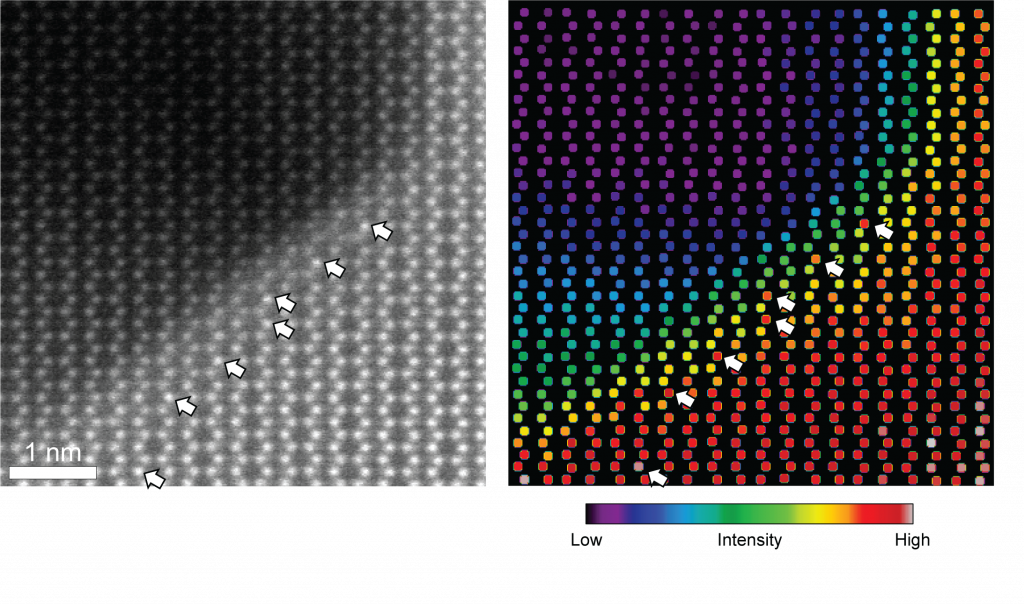
Point defects play a key role in determining the properties of nearly all materials, from electron and ionic transport to radiation effects in structural materials. Detection of individual point defects has been a long-sought-after goal in transmission electron microscopy. However, detection of point defects, especially, isolated light elements or vacancies, is a formidable challenge due to the limited detection efficiency and inherent noise in modern transmission electron microscopy.
Our group focuses on the development of novel TEM imaging and data analysis techniques with atomic-scale spatial resolution, high measurement precision, and single-atom sensitivity to enable the detection of point defects, revealing their effects on local structure and symmetry, and unveiling the structure-property correlation.
Potential application of these techniques to new functional materials will resolve key questions, such as the microscopic origin of the limited dopant activation in new transparent conduction oxides, or the role of point defects and surface structure in perovskite quantum dots.
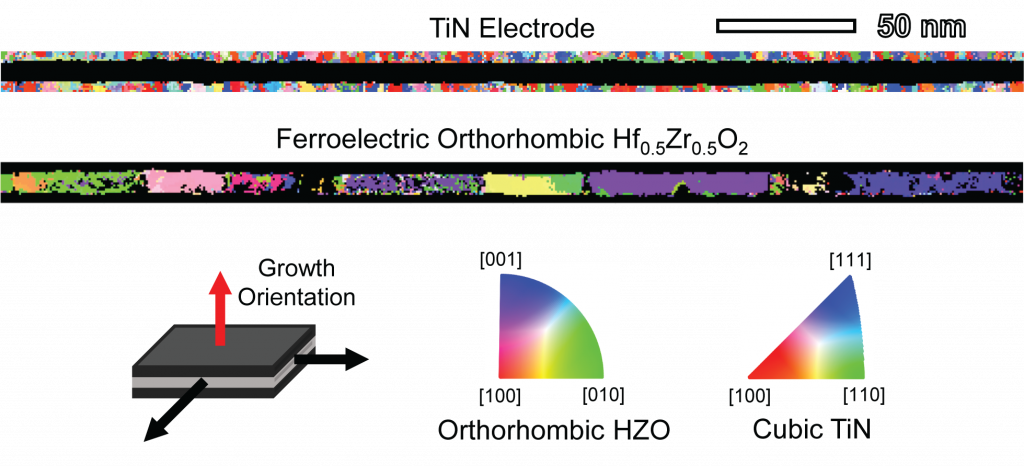
Topic 2: Polarization Switching Dynamics in Ferroelectric Thin Films
Every year, the amount of stored and processed digital information continues to grow significantly. This trend is further accelerated by the recent development of data-intensive computing technologies such as artificial intelligence (AI). To keep pace with the ever-increasing data, there is a critical need to develop (1) novel computing systems with low power consumption and efficient data processing and (2) memory devices with high data capacity and fast read/write speed, and non-volatility. Ferroelectric materials (in thin-film form) have gained tremendous interest as candidates for next-generation synaptic devices that serve as memory units in neuromorphic computing systems.
Our group focuses on uncovering the mechanisms of ferroelectric domain formation and polarization switching dynamics using advanced imaging methods in TEM (e.g., in situ biasing and 4D-STEM). The materials system that we are currently working on includes Zr-doped hafnia, ScAlN, and improper ferroelectric materials (.e.g., YMnO3).
Topic 3: Defects in Ultra-Wide Bandgap Semiconductors for Power Electronics
Semiconductors with wide bandgaps and excellent transport properties can withstand high electric fields and currents, and offer high switching speed, thus making them ideal platforms for next-generation power electronics. Power devices typically operate in harsh environments (e.g., high electric fields); as a result, defects can nucleate, evolve, and interact by external stimuli under realistic operation conditions. Thus, it is critical to characterize crystal defects and produce a fundamental understanding of the effects of defects on materials properties and device performance. Our group currently focuses on characterizing defects in beta-phase gallium oxide in order to elucidate the mechanisms of defect formation and electrical activity.
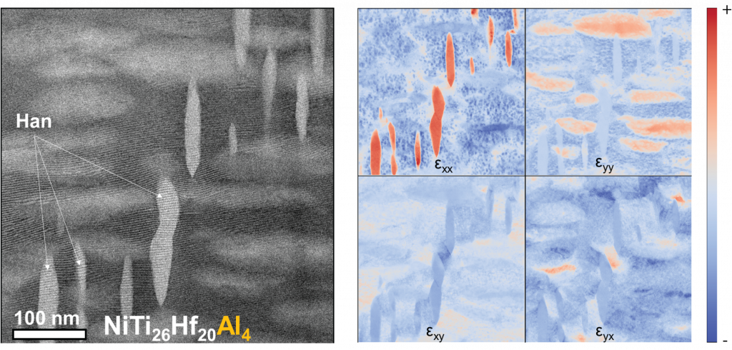
Topic 4: Shape Memory Alloys
Shape memory alloys exhibit the unique and interesting property of recovering their original structure after severe deformation. This is achieved through a phase transition that occurs with the application of heat. In particular, NiTiHf-based shape memory alloys have attracted much interest for their great precipitation strengthening and high transition temperature. This makes them ideal for applications in the aerospace and automotive industries for essentially any component that would be subject to high temperatures and work loading. More recent efforts have involved including small percentages of aluminum in these alloys, resulting in a coprecipitation phenomena that greatly increases strength at the cost of lowering transition temperature. Thus, it is vital to systematically investigate the precise mechanisms by which these competing precipitates form and affect the microstructure as a function of formation and aging conditions. STEM is an ideal tool for detailing the functional maps across the atomic-to-microscale regime to understand which phases form preferentially, their relative volume fractions, and the strain fields that arise as a consequence of these coexisting, complex structures.
Topic 5: Computer-Vision and Machine-Learning Enabled TEM Data Processing
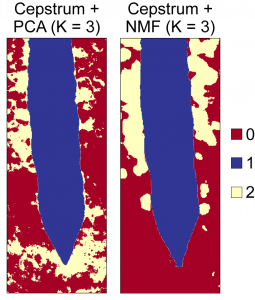
Nowadays, with the advent of the direct electron detector featuring high readout speeds and dynamic electron count range, the availability and speed of acquiring diffraction data in the microscope is unparalleled. This is done using a popular technique called four-dimensional (4D) STEM, where a 2D electron diffraction pattern is collected at every scan position in a 2D field-of-view (hence, 2D + 2D = 4D). Thus, the main hurdle with such a plethora of data lies in the subsequent data analytics and how to efficiently and accurately quantify properties of interest from them. Digital image processing techniques, such as template matching and Gaussian peak fitting, are ideal for capturing diffraction spots to collect their intensities and measure reciprocal space vectors for strain mapping. However, when a typical 4D-STEM dataset can hold 10-100 thousand diffraction patterns, these basic methods become impractical. Consequently, recent efforts have looked towards machine learning-guided data analysis methods, especially in convolutional neural networks and unsupervised machine learning. Our group is currently working on developing novel unsupervised machine learning procedure for analyzing these large 4D-STEM datasets in an efficient and accurate manner without the need to label the data or provide any user interference.